
PLA / ROM
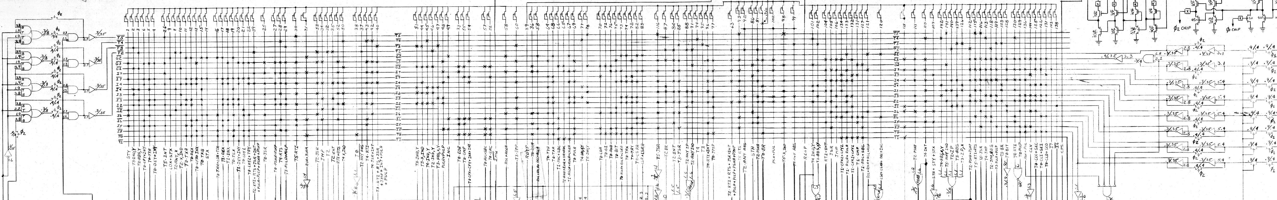

Unlike the original 6502 (pictured above), the lines / logic will be organized regardless of space for clarity, much like GitHub user davidmjc did for his schematic[github.com] , which I highly recommend playing around with.
Because of performance reasons, each section has to be a component. Because of size limitations of components, the PLA has been split into 3 sections which will be wired together: A,B,C - D,E,F - G,H,K. The order of the wires, top-to-bottom, is as follows:
T5,T4,T3,T2,R01,R0!,R1!,R2,R2!,R3,R3!,R4,R4!,R5,R5!,R6,R6!,R7,R7!,T1,T0,TA,TM,TW
The anomalies: R01, R0!, R1!
The first bit is R0 OR R1. The reason these bits are set apart are because the OP codes are distributed CCAAABBB, where A and B are essentially "Row / Column" and C is "Page." As for why the top bit isn't a NAND or AND, that could be because I am simplifying NAND and NOR to AND and OR. I haven't looked into it yet, but this might indicate the top bit should to be a NOR. If that were the case, then this would behave much like a half adder without a sum bit. To make a half adder behave like a decoder, you would just have to add a switch to whatever line you want. However, many lines ignore the C bits.
TA/TM/TW
I haven't looked into it yet, but I know these are related to the cycle counter.
T0-T5
These are related to the timing control. How you can get 6 unique outputs from two clocks is something I haven't looked into yet.
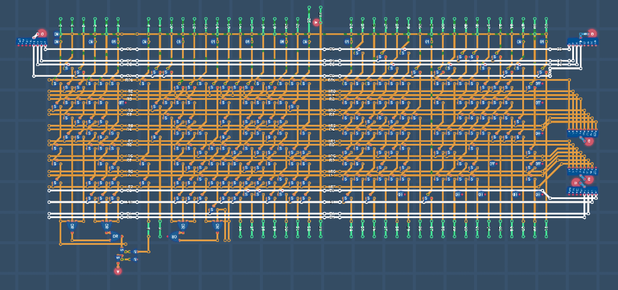
Progress: (As of 10/30/23)
A-C:
As you can see, I started adding some output logic at the bottom. This is when I decided I needed to document and publish the work so other people may be able to point out any mistakes, as I can barely read transistor level logic.
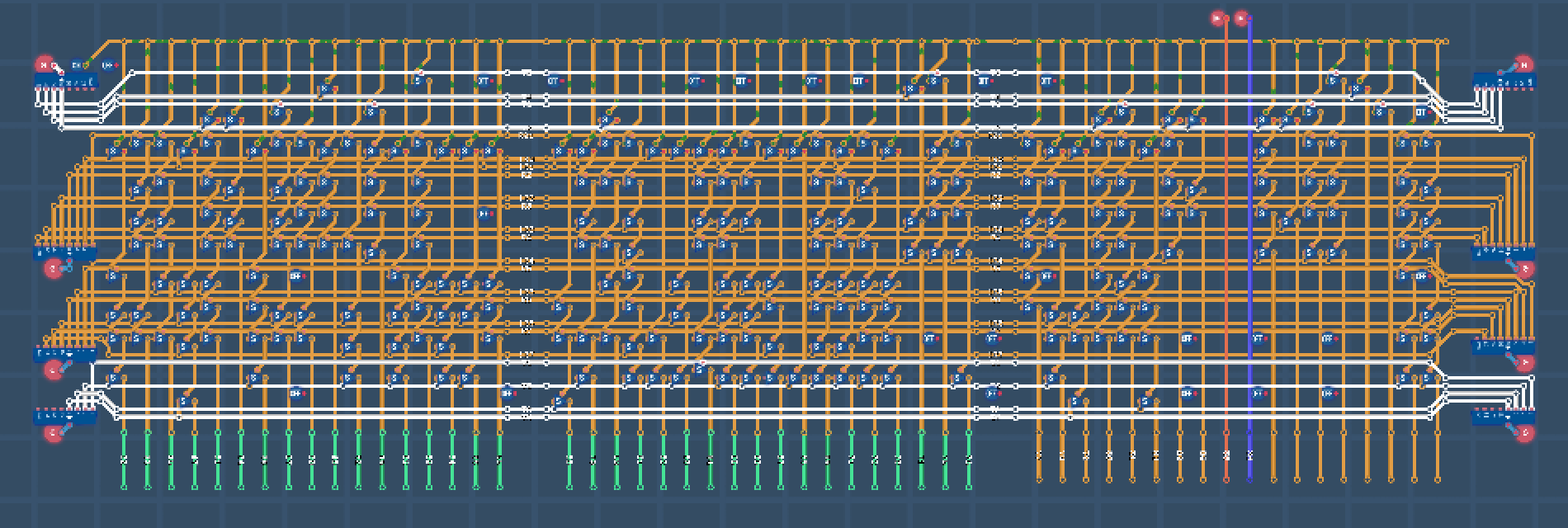
D-F:
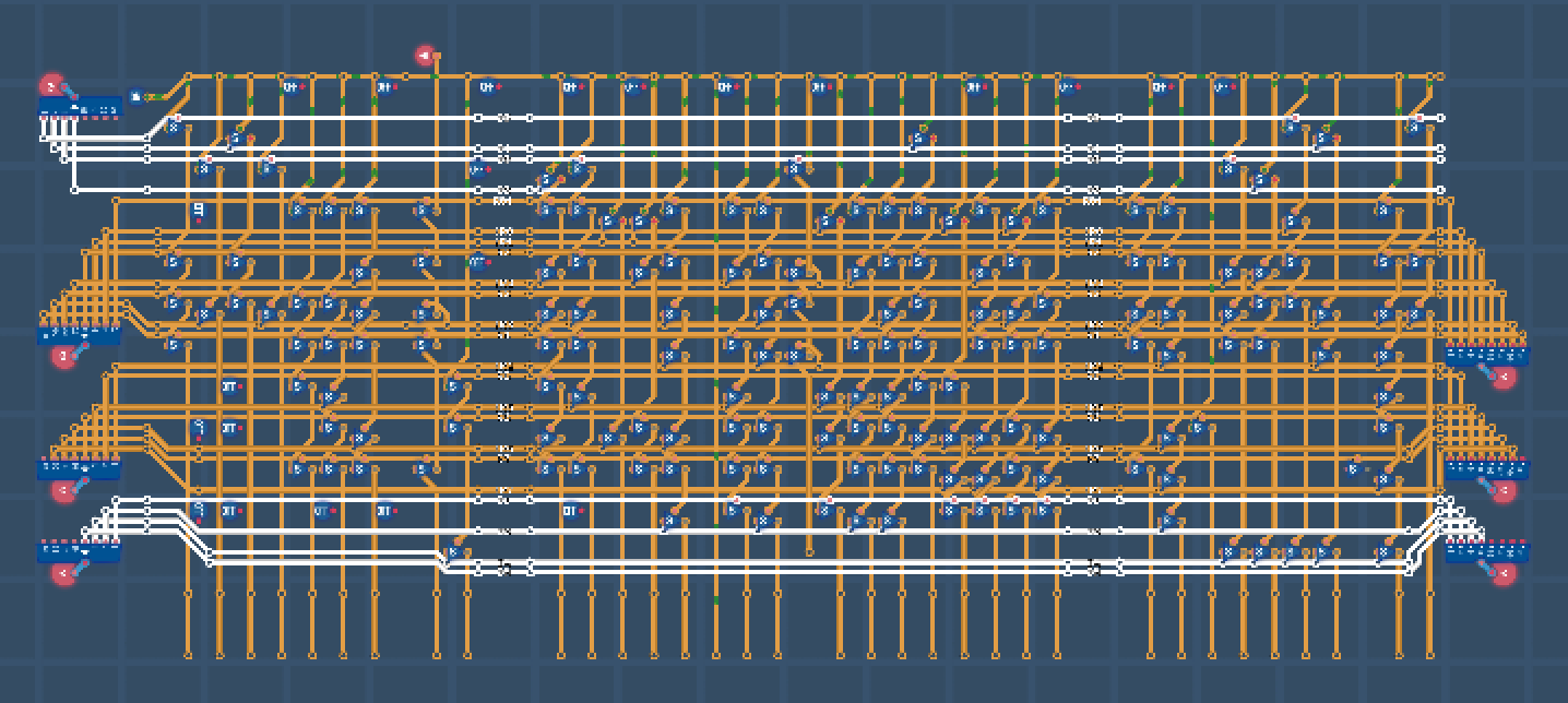
G-K:
This is the component shape so far:
Please let me know if I made any mistakes or you have any corrections in my terminology. I am mostly reiterating what I think I understand from a whole lot of reading.
Precode / Instruction Register
TODO: WIP
Data Path Controller
TODO: WIP
Interrupt Control
TODO: WIP
Timing Control
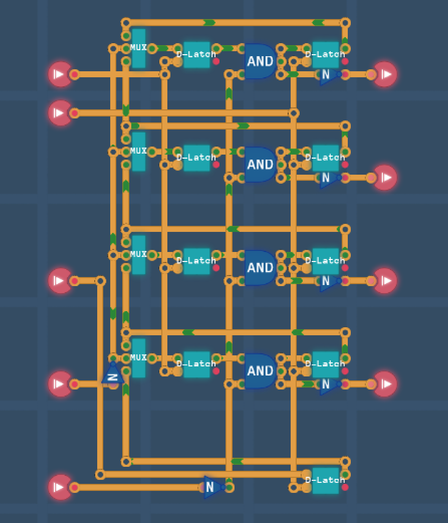
After a few hours of blankly staring at schematics and reading the same paragraph over and over, I finally figured out how the timing control works. I think.
If you are at all familiar with the data sheet of the 6502, you would know that each operation takes at least 2 cycles to complete. Specifically, they can take anywhere between 2 and 6 cycles, with an additional cycle depending on certain conditions - usually when data overflows between 'pages'. How does the 6502 know how long each operation should take? Well the timing controller, of course.
The 650X clocks are described as "two phase non-overlapping." This means that each clock step is separated into two, half cycles, Phi 1 and Phi 2. When both of these have pulsed, the T value should increment once, indicating the next step in the operation. When an operation is complete, the processor sends a reset pulse so the timing control circuit so it is ready for the next instruction.
Additionally, a 1 bit multiplexer is used for the ready signal so when it is high, the output of each D-Latch is fed back into itself, stoping the incrementation until the processor is ready. This is an active low input, so it is inverted.
Here is the component:
The D-Latches are a NOR Flip-flop with a delayed output. The delay is necessary to prevent circular dependency. However, this does mean the counter takes a tick to initialize.
You might notice the component does not isolate the output. This is because the operation decoder isolates the line in it's logic. This does not make the opcode logic easier or faster, but it does save having to group each instruction by the required length of the instruction.
There are two other timing controller circuits that I have not made yet. T0-1 and TA-W. T0 and T1 are used for short instructions. They are separated from T2-5 because the minimum cycle count is 2 and this is the delay of most operations. TA, TM, and TW are used for long instructions. I believe that controller should only ever add 1 cycle, but the labels, A, M, and W, are related to why the additional cycle is required.
Decimal Adjust Accumulator
TODO: WIP
Accumulator Register
TODO: WIP
Index X And Y Registers
TODO: WIP
Program Counter Low / High Registers
TODO: WIP
ALU
TODO: WIP
Source: https://steamcommunity.com/sharedfiles/filedetails/?id=3067097737
More Turing Complete guilds
- All Guilds
- Turing Complete Guide 202
- Turing Complete: Basic Logic-Manual
- Robot Racing
- Turing Complete: Basic Logic-Solution
- Turing Complete: CPU Architecture-Solution
- Turing Complete: Arithmetic and Memory-Solution
- Turing Complete: All-level walkthrough
- Turing Complete Guide 157
- / Turing Complete